- 您现在的位置:买卖IC网 > Sheet目录1995 > DS4302Z-020/T&R (Maxim Integrated Products)IC DAC 5-BIT SGL 0-2.0V 8-SOIC
DS4302
2-Wire, 5-Bit DAC with Three Digital Outputs
2
_____________________________________________________________________
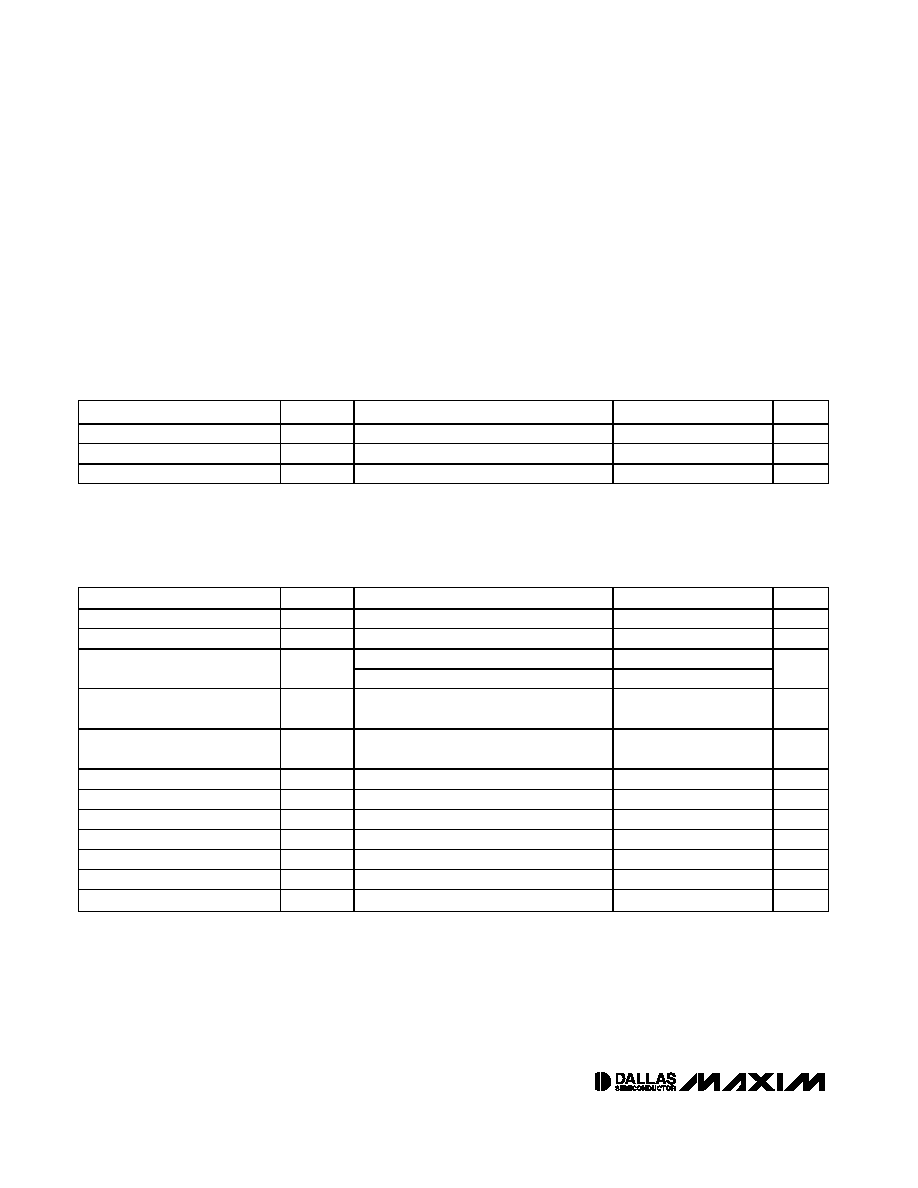
ABSOLUTE MAXIMUM RATINGS
RECOMMENDED DC OPERATING CONDITIONS
(TA = -40°C to +85°C)
Stresses beyond those listed under “Absolute Maximum Ratings” may cause permanent damage to the device. These are stress ratings only, and functional
operation of the device at these or any other conditions beyond those indicated in the operational sections of the specifications is not implied. Exposure to
absolute maximum rating conditions for extended periods may affect device reliability.
Voltage Range on VCC, SDA, and SCL Pins
Relative to Ground.............................................-0.5V to +6.0V
Operating Temperature Range ...........................-40°C to +85°C
Storage Temperature Range .............................-55°C to +125°C
Soldering Temperature.....See IPC/JEDEC J-STD-020A Specification
PARAMETER
SYMBOL
CONDITIONS
MIN
TYP
MAX
UNITS
Supply Voltage
VCC
(Note 1)
4.5
5.5
V
Input Logic 1 (SDA, SCL)
VIH
2.0
VCC + 0.3
V
Input Logic 0 (SDA, SCL)
VIL
GND - 0.3
0.8
V
PARAMETER
SYMBOL
CONDITIONS
MIN
TYP
MAX
UNITS
Standby Current
ISTBY
(Notes 2, 3)
200
300
A
Input Leakage
IL
(Note 4)
-1.0
+1.0
A
3mA sink current
0.0
0.4
SDA Low-Level Output Voltage
VOL1
6mA sink current
0.0
0.6
V
P0, P1, P2 Low-Level Output
Voltage
VOL2
(Note 1)
4mA sink
+0.4V
V
P0, P1, P2 High-Level Output
Voltage
VOH
(Note 1)
4mA source
VCC - 0.4V
V
VOUT Maximum Level (-020)
VCC = 5.0V, Data = 00000XXX (Note 3)
1.925
2.0
2.075
V
VOUT Minimum Level (-020)
VCC = 5.0V, Data = 11111XXX
0.0
0.05
0.1
V
VOUT Maximum Level (-019)
VCC = 5.0V, Data = 00000XXX (Note 3)
1.825
1.9
1.975
V
VOUT Minimum Level (-019)
VCC = 5.0V, Data = 11111XXX
0.0
0.05
0.1
V
Power-On Reset
1.7
V
Settling Time
10
s
D/A Output Levels
32
steps
DC ELECTRICAL CHARACTERISTICS
(VCC = +4.5V to 5.5V, TA = -40°C to +85°C.)
X = Don’t care.
发布紧急采购,3分钟左右您将得到回复。
相关PDF资料
DS4302Z-020+
IC DAC 5-BIT SGL 0-2.0V 8-SOIC
DS4311P+
IC OSC CLOCK 311.04MHZ 10-LCCC
DS4404N+
IC DAC 4CH I2C ADJ 14-TDFN
DS4412U+
IC DAC DUAL CH I2C ADJ 8-USOP
DS4424N+
IC DAC 7BIT 4CH 5.5V 14-TDFN
DS4425BN+
IC OSC CLOCK 425MHZ 10-LCCC
DS4426T+T&R
IC DAC I2C-MARGINING 4CH 28-TQFN
DS4432U+
IC DAC 7BIT 2CH 5.5V 8-MSOP
相关代理商/技术参数
DS4302Z-020+
功能描述:数模转换器- DAC 2-Wire 5-Bit w/3 Digital Outputs RoHS:否 制造商:Texas Instruments 转换器数量:1 DAC 输出端数量:1 转换速率:2 MSPs 分辨率:16 bit 接口类型:QSPI, SPI, Serial (3-Wire, Microwire) 稳定时间:1 us 最大工作温度:+ 85 C 安装风格:SMD/SMT 封装 / 箱体:SOIC-14 封装:Tube
DS4302Z-020+T&R
制造商:Maxim Integrated Products 功能描述:DAC 1CH 5-BIT 8SOIC N - Tape and Reel 制造商:Maxim Integrated Products 功能描述:IC DAC 5-BIT SGL 0-2.0V 8-SOIC
DS4302Z-020+T&R
功能描述:数模转换器- DAC 2-Wire 5-Bit w/3 Digital Outputs RoHS:否 制造商:Texas Instruments 转换器数量:1 DAC 输出端数量:1 转换速率:2 MSPs 分辨率:16 bit 接口类型:QSPI, SPI, Serial (3-Wire, Microwire) 稳定时间:1 us 最大工作温度:+ 85 C 安装风格:SMD/SMT 封装 / 箱体:SOIC-14 封装:Tube
DS4303
制造商:MAXIM 制造商全称:Maxim Integrated Products 功能描述:Voltage Sample and Infinite Hold
DS4303K
功能描述:电源管理IC开发工具 RoHS:否 制造商:Maxim Integrated 产品:Evaluation Kits 类型:Battery Management 工具用于评估:MAX17710GB 输入电压: 输出电压:1.8 V
DS4303R/R
制造商:MAXIM 制造商全称:Maxim Integrated Products 功能描述:Voltage Sample and Infinite Hold
DS4303R/T
制造商:MAXIM 制造商全称:Maxim Integrated Products 功能描述:Voltage Sample and Infinite Hold
DS4303R/T&R
制造商:Maxim Integrated Products 功能描述:NV ADJ VOLTAGE REFERENCE SOT23-5 - Tape and Reel